SiDi128 — FPGA COMPUTER
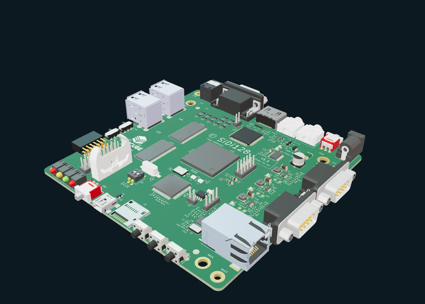
SiDi-128 motherboard, rendered from native CAD on a dark studio floor

PRECISION ARRAYS / THE SIDI-128 PROJECT

Small board.
Entire worlds.

Reconfigurable hardware.
Connections across generations.

A Cyclone 10 FPGA, 128 MB of SDRAM, and a rich mix of classic and current interfaces. Meet the board at the heart of SiDi-128.

FPGA / SDRAM / RETRO COMPUTINGDevelopment hardware
01 — THE IDEAScroll to discover ↓Native CAD · Blender studio render
10CL120Intel Cyclone 10 LP FPGA
128 MBTwo SDRAM devices
125 × 125Board footprint · millimetres
08Copper layers

02 / HARDWARE EXPLORER

Turn it around.
Take it apart.

Explore the native KiCad board and separate its component groups. Switch to printed R18 or FR4-R7 to lift the lid and reveal the enclosure assembly.

SIDI-128 / NATIVE BOARDThe heart of the project.125 × 125 mm PCB · eight copper layers
Preparing the hardwareLoading native CAD geometry…
Native KiCad geometry
Drag to orbit · Scroll / pinch to zoom · Right-drag to pan
Current PCB, including the revised connector positions and four fiducials.Geometry exported from the saved design

The board Inspect the native board, or separate its component groups.

Printed R18 Four removable faceplates and an eight-screw lid.

FR4-R7 Six panels, metal posts and countersunk fasteners.

03 / THE ARCHITECTURE

Reconfigurable by design.
Connected by purpose.

Follow the design from programmable logic and memory to picture, sound and the connections around the board.

SIDI-128 / FUNCTIONAL DESIGNPROGRAMMABLE CORE
Functional paths · selected interfaces shown

The Cyclone 10 FPGA connects to two SDRAM devices, dedicated clocks and the ATSAMV71 controller.

FOLLOW THE DESIGN

The core is yours to define.

The Cyclone 10 LP FPGA connects to two SDRAM devices, with dedicated clocks and an ATSAMV71 controller.

FPGA cores and firmware determine the behaviour of the system.

One compact board.
Distinct roles, working together.

Explore a functional view of the design, then return to the native model to see the components themselves.

BENEATH THE COMPONENTS

Eight layers.
A foundation for every signal.

Signal routing, ground references and power share a carefully defined stack. Three internal ground layers provide reference planes within the board.

Signals Ground Signals / power
Open the native stackup drawing ↗
PCB CROSS-SECTIONTOP ↓ BOTTOM
  1. 01F.CuSignals / components
  2. 02In1.CuGround reference
  3. 03In2.CuSignals
  4. 04In3.CuGround reference
  5. 05In4.CuSignals / power
  6. 06In5.CuSignals
  7. 07In6.CuGround reference
  8. 08B.CuSignals / components
Dielectric separates the copper layers · thickness exaggerated

04 / THE ENCLOSURES

One board.
Two ways to build around it.

Two distinct constructions, both following the October 14 board. Explore their current geometry and see how each enclosure comes together.

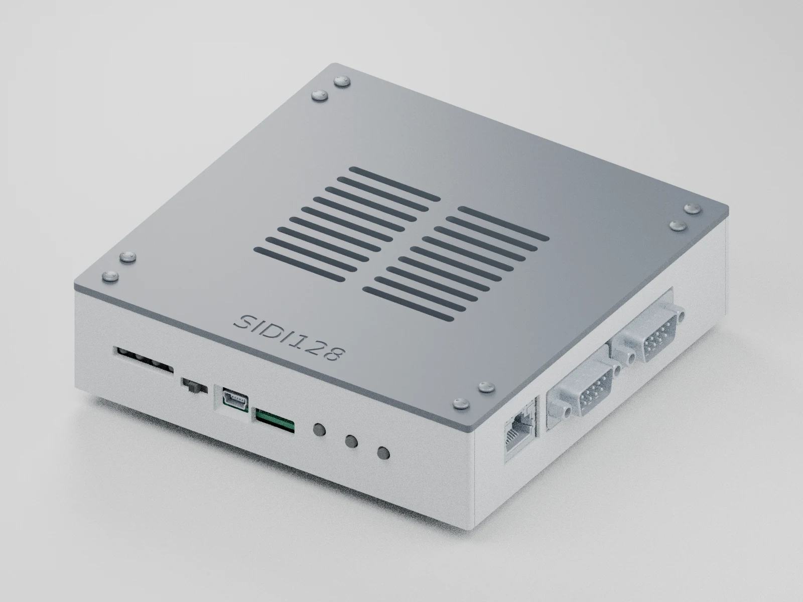
Current printed R18 case with vented lid and eight lid screwsPRINTED / R18

PRINTED PARTS · HEAT-SET INSERTS

A case made to come apart.

A compact printed base, four removable faceplates and a reinforced, vented lid. Two upper mounts on each faceplate secure the lid on all four sides.

Printed body
131.8 × 131.8 × 34.9 mm
Fasteners
20 × M2.5 inserts and screws
Lid attachment
Eight M2.5 screws
Read the assembly notes ↗
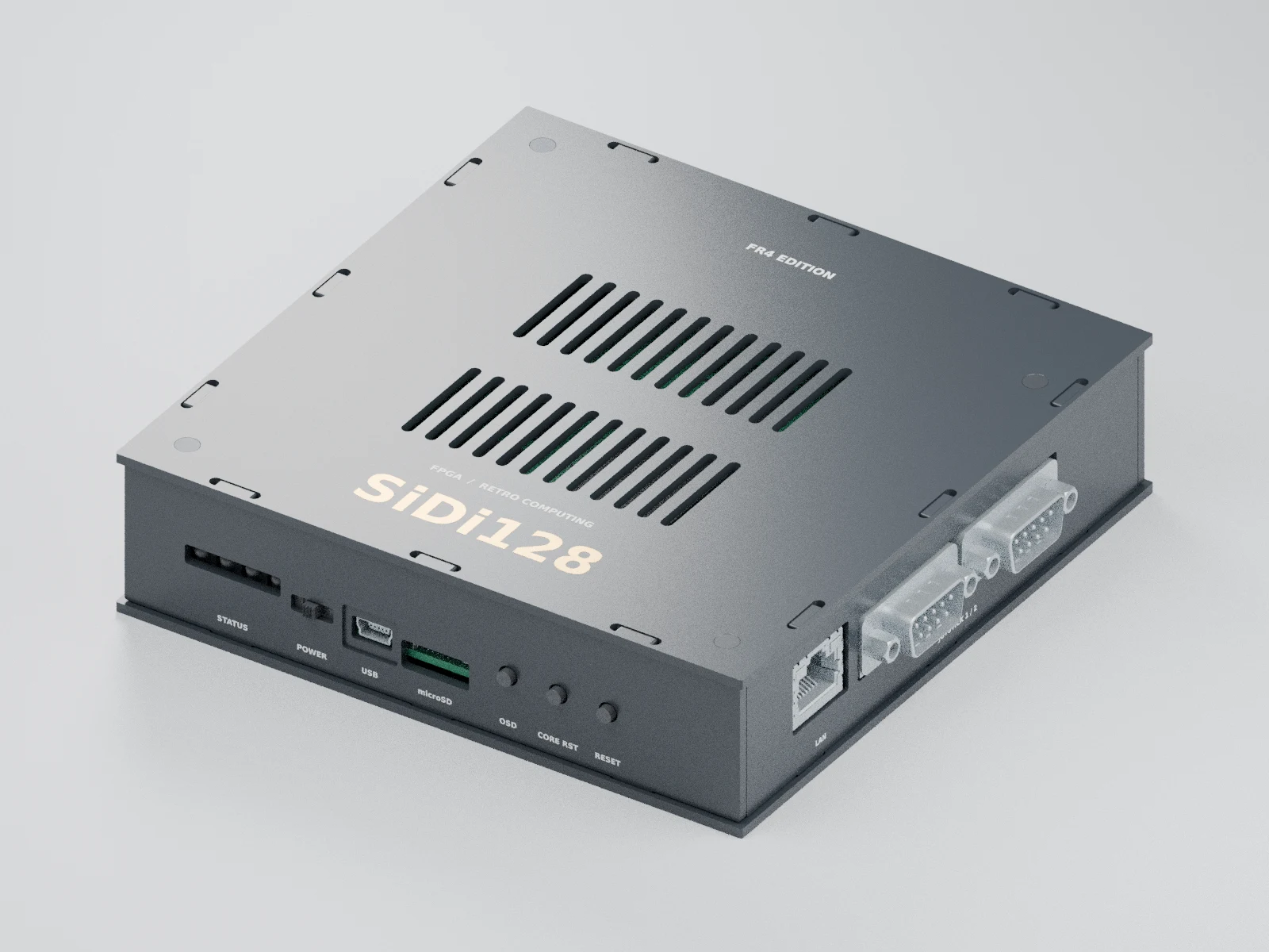
Current FR4-R7 enclosure with tabbed panels, vented lid and SiDi128 letteringFR4 PANELS / R7

FR4 PANELS · METAL STANDOFFS

Six panels. A precise stack.

Six 2 mm FR4 panels meet at captured tabs. Two-piece metal post columns clamp the PCB, while separate countersunk screws secure the base and lid.

Panel envelope
133 × 133 × 33.6 mm
Construction
FR4 panels + M2.5 metal posts
Lid attachment
Four countersunk screws
Read the assembly notes ↗
CURRENT PORTS

Access on every side.

Both cases follow the revised board’s connectors, switches and microSD position. The 3D explorer shows the complete board inside each enclosure.

100 × 100 MM MOUNTING GRID

Open the lid. Mount the base.

Three base mounting axes follow the VESA grid. Remove the lid for screw access, fit the monitor mounting hardware, then refit the lid.

Current CAD prototypes: printed R18 and FR4-R7. Dimensions exclude projecting connectors and external mounting spacers. Physical fit, thermal behaviour and mounting strength still need qualification. FR4 machining details are in the fabrication notes ↗.

05 / THE ASSEMBLY BOOK

Good design.
Down to the details.

Start with top assembly, then turn the board over and explore its stackup, routing and power guides.

Open the 5-page board guide ↗

SELECT A DRAWING

Native engineering drawings
Development documentation

01 / 05

Board / top assembly

06 / WHERE WE ARE

Real hardware.
A continuing story.

CURRENT BOARD SNAPSHOT

SiDi-128 / V1.1

The October 14 layout, with revised port positions and four fiducials. The board model matches the saved KiCad PCB on GitLab.

Native geometry throughout the interactive explorer.
CURRENT ENCLOSURES

R18 + FR4-R7

Printed and FR4 approaches, each with a vented lid, serviceable panels and mounting access through the open top.

Current models replace the earlier enclosure study.
NEXT CHAPTER

Build. Test. Refine.

Physical assembly, connector access, firmware and core support, thermal checks and mounting validation.

Development models are separate from production qualification.
SiDi—128

Small board. Entire worlds.

Explore the hardware ↑
Assembly drawingOpen PDF ↗
Enlarged assembly drawing

Use the PDF for vector detail and printing.