
Six SRAM chips share a 16-bit bus, while the Amiga AGA chipset needs each word at a precise clock edge. This technical walkthrough follows the AmiCube SRAM port from graphical corruption to a working memory architecture.
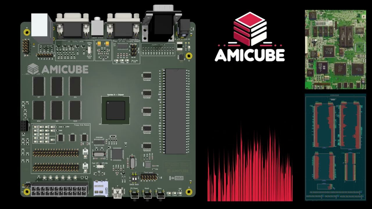
About this video
The investigation covers predictive DMA scheduling, bus ownership, the TG68 cache, physical memory writes and the timing limits behind a nominal 10 ns SRAM rating. A fourth-word AGA failure shows why enough overall bandwidth is not sufficient when a graphics fetch arrives one edge late.
The later sections examine the C102 scheduler, physical CPU and PiStorm clocks, and the ARM/FPGA firmware interface. At the time of recording, C102 was a promising candidate with encouraging hardware results; extended testing, electrical margins, socket-mode operation and final performance qualification were still in progress.